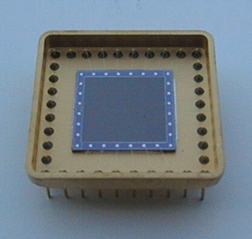
A CCD IC (Integrated Circuit). The sensitive area is the bluish-black area. Very small bonding wires link the silicon chip to the pins of the package.
A CCD detector (Charge Coupled Device) consists basically in a photo-electrically sensitive plane area. This detector is positioned at the focal plane of an optical instrument. For example, in place of a photographic film which is photo-chemically sensitive. The basic material of the photosensitive area of the CCD is silicon. It is doped in order to embue it with photoelectrical properties. As a result, when this photosensitive area absorbs a photon (elementary piece of light energy), there is a good chance that it will produce an electric charge, an electron.
Looking at the photosensitive area of a CCD though a microscope, a network of tiny electrically independent cells can be seen. These cells are called photosites or pixels, with size ranging from a few microns to a few tens of microns depending on the IC. If they are electrically polarised correctly, (supplying adequate voltages) each photosite is able to gather a large number of the electrons that the incident light flux generate on this photosite. The number of electrons is directly related to the brightness of the incident light flux for the concerned photosite and to the duration of exposure. For example, if the time of exposure to a given light flux is doubled, the number of electrical charges generated at the photosite will also be doubled. We find here the concept of exposure time well known in photography.
The conversion rate of the photons into electrons (electric charges) is called the quantum efficiency. The quantum efficiency is largely dependent on the wavelength of the incident light; it defines the sensitivity of the CCD in a spectrum domain, (most of the time from 0,4 to 1 micron wavelengths). For wavelengths where the CCD sensitivity is maximum, usually deep red, the quantum efficiency is about 40 to 50% for general purpose CCDs, but quantum efficiency up to 90% can be reached for optimised (and costly) CCDs !

The CCD is delivered in a standard IC (Integrated Circuit) package, with one particularity, the top cover is transparent to the light (a small glass window protects the sensitive area from dust and the very small bounding wires around the sensitive area from being torn out).
During the exposure to light, the optical image is converted into electronic
charges and thus into an electronic image. The smaller the size of the
photosites, the smaller the sampling (or the resolution) of the electronic
image. So the electronic image may have the capability to represent accurately
very small details of the optical image.
The photosites are also called pixels (picture element).
In fact the pixel is rather the result of the sampling of the signal acquired
by a photosite. In the books, the word pixels and photosites are often
used one for the other, and we will contribute also to this mix in this
documentation !
There are physical limits to the size of the photosites (5 to 6 microns at the smallest) and limits due to performances. If the photosites are too small, the quantity of electrical charges storable into a photosite becomes too small to provide a large enough dynamic range necessary for scientific use of the image. Large pixels (30*30 microns) can collect a large number of electric charges but will have a poor image resolution - at least with most of the usual optical configurations.
A CCD matrix may have lines and/or columns with several hundred or even thousands of pixels.
After the exposure, the signal integrated at each photosite has to be transferred line by line, and then for the bottom line, column by column to the output amplifier. Finally, a pin of the CCD IC delivers sequentially the electrical analogue information concerning the charge of all the photosites.
The line by line transfer of the photosites, called vertical transfer, is performed by a sequential appropriate polarisation of the lines of pixels. The sequential polarisation is done using vertical clock signals. With an adequate clock cycle, the electrical charges of a line of photosites are transferred to the line just below (next line - traditionally the charges are considered as travelling from the "top line" to the "bottom line" of the CCD). By the same process, the last line (at the bottom) is transferred to a special line called a horizontal transfer register. The next Figure illustrates the transfer mechanism.

Once the electrical charges of the photosites of one line are emptied into the horizontal transfer register, it is the right time to read this register. For that, a second set of clock signals (the horizontal clocks) is activated to achieve the transfer of the charges along the horizontal transfer register. When the charges corresponding to one photosite arrive at the end of the register they are sent to an electronic network into the CCD IC to convert the electric charges into electrical voltage. This network proceeds in three steps : (1) a capacitor is loaded to a predefined value, called the precharge value, by closing a switch to apply to the capacitor a fixed voltage (a specific clock is needed for that). (2) The switch is opened; a small variation of the capacitor voltage, very similar to a noise, may result from opening the switch. (3) The negative electric charges from a photosite are injected into the capacitor; resulting in a discharge of the capacitor. The change of the voltage of the capacitor is strictly proportional to the number of electrons of the transferred photosite, and thus, to the charge of the corresponding photosite.

After being amplified the voltage is delivered on a pin of the IC. So, as the reading proceeds as dictated by the cycles of the clocks, the output pin of the CCD streams the information about the quantity of electrical charges (and thus of light) at each photosite. This signal is called the video signal. The output stage, where all the information contained in the image transits, is the actual bottleneck of the data flow. The overall time to read the electronic image depends upon the clock frequencies. For a camera with about 400 000 pixels, optimised to detect low light power flux, the reading time may require several seconds.
At this stage, an electronic network, external to the CCD IC, amplifies, reshapes, converts to digital, and transfers the numeric data of each photosite to the PC. The conversion of the continuously variable signal coming from the CCD from analogue to digital is mandatory because the computer understands only binary numbers. The analogue video signal conversion into binary data coding is generally done in 8-bits words or better, 16-bits words. The computer rebuilds the image on the screen point by point (pixel by pixel), in grey levels, in colours or any other way. Also the computer saves the precious data of each photosite into the mass memory for later processing.
One very appreciated characteristic of the CCD and of the network associated to the CCD IC is that it only adds a very small amount of noise to the useful video signal. The noise is a random variation added to the actual signal which can be so high than the useful signal is totally scrambled. The noise limits the sensitivity of the sensor, in simple words: it limits the capability to detect faint objects. In general, the unit used to describe the level of noise is the equivalent number of electrons at the output stage of the CCD. A noise below 20 electrons characterises a camera used for very low light flux detection, as is often the case for astronomical cameras. However, it is not the only parameter by which to judge the overall performance of a CCD camera. The quantum efficiency is a major parameter to evaluate the overall sensitivity of the detector. The quantum efficiency is the ratio of generated electron charges to the number of incident photons. For most of the current (- reasonable cost) CCDs, the quantum efficiency is between 30 and 40% (largely dependant on the wavelength). Another interesting characteristic is the linearity of the response (proportionality over the full range between the number of received photons and the electrical signal observed at the output of the CCD or of the digital value at the output of the camera). For example this allows accurate photometry measurements. Usually linearity is excellent for CCDs.
The image transferred from the camera, directly stored in the computer
memory is called the raw image. It consists of the image data itself, and
spurious signals. In particular, in the spurious signal, there is an
offset
signal due to the electronic elements integrated within the CCD and possibly,
from the external video processing networks. Another spurious signal is
the thermal noise, which spontaneously appears at each photosite
while it is integrating the actual signal of the image. The random motions
of the electrons within the chip generate spurious electric charges that
produce this thermal signal, also called dark signal.
Even when the CCD is completely in the dark, the dark signal is present
and produces a detectable electric signal. As is the case for the useful
signal, the dark signal is proportional to the exposure (also called integration)
duration. The dark signal can dominate the useful signal if no specific
measures are taken. The only solution to decrease the dark signal production
rate is to decrease the CCD temperature when it's operating.
In the first phase of the image processing, all the additive spurious
signals have to be eliminated, as far as possible. This rather critical
phase is called preprocessing. The preprocessing corrects not only
the additive spurious biases but also the multiplicative biases. The multiplicative
biases are due to the fact that all the pixels have not exactly the same
sensitivity and that the efficiency of the instrument for transmission
of the light is not identical for all the pixels, (as example vignetting).
Also dust particles, if present on the CCD window will intercept some light.