TESTS WITH AN OSCILLOSCOPE
Audine doesnt need to be adjusted with an oscilloscope : the following
information apply essentially to the specialists who want to observe how
their camera internally operates.
The timing diagrams which illustrate this chapter show the look of the
signals at some strategic points of the electronic circuit. To produce
them, it is necessary to launch special commands from the console mode
of PISCO. Two
commands are used : TEST and TEST2 :
Command TEST [NUMBER]
This command executes NUMBER transfer cycles
from the image area to the horizontal register. The following sequence
of instructions describes each basic cycle (for further explanations, click
here):
_asm
{
mov dx,base
mov al,11111011b
out dx,al
out dx,al
out dx,al
out dx,al
out dx,al
out dx,al
out dx,al
out dx,al
mov al,11111010b
out dx,al
out dx,al
out dx,al
out dx,al
out dx,al
out dx,al
out dx,al
out dx,al
mov al,11111001b
out dx,al
out dx,al
out dx,al
out dx,al
out dx,al
out dx,al
out dx,al
out dx,al
mov al,11111010b
out dx,al
out dx,al
out dx,al
out dx,al
out dx,al
out dx,al
out dx,al
out dx,al
mov al,11111011b
out dx,al
out dx,al
out dx,al
out dx,al
out dx,al
out dx,al
out dx,al
out dx,al
}
The code sets the clocks V1 and V2 in action, and performs the
charge transfer from the image area. As the code is very short, it complies
very quickly too. So to observe the clocks V1 and V2 with the oscilloscope
a long time enough, you must give the argument NUMBER
a big value. Try for instance :
TEST 10000
Command TEST2 [NUMBER]
This command executes NUMBER cycles of
quick reading of the camera. The following sequence of instructions describes
each basic cycle :
for (i=0;i<521;i++)
{
zi_zh(base);
for
(j=0;j<790;j++)
{
_asm
{
mov dx,base
mov al,11110111b
out dx,al
mov al,11111111b
out dx,al
out dx,al
out dx,al
mov al,11111011b
out dx,al
out dx,al
out dx,al
}
}
}
This code activates all the clocks that command the CCD (clocks V1,
V2, H1, H2, R). The TEST2 command is particularly aimed to examine
the look of the video signal at the pixel level. For instance, to observe
3 successive frames, you will execute :
TEST2 3
The two following pictures show the look of the video
signal for two different lighting levels after the coupling capacitor
C1 ,on the pin 3 of the circuit U6 (the quad amplifier AD713). To see these
timing diagrams, you must launch the TEST2 command from the PISCO
console.
Nota : It is very dangerous to observe the video signal directly
at the CCD output (on pin 2). The least shortcut between this pin and its
neighbors can destroy the CCD internal output amplifier. Record the video
signal in these conditions only with a special care and if it is really
necessary. By measuring the video signal after the coupling capacitor C1
, as recommended before, you will protect the output amplifier of the CCD.

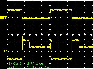
Video signal on the pin 3 of U6 (input of the amplifying chain).
The CCD is lighted so as the pixels are saturated. The first timing
diagram (canal 1) is a synchronization signal, taken on the pin 1 of U4
(MAX333A). It is the command signal P3, which produces the CCD clocks H1
and H2.
The second timing diagram (canal 2) is the actual video signal.
It is easy to distinguish the reset stage, the reference stage and the
video stage (this one with the lowest level). The little arrow marked 2,
on the left side of the picture, indicates the ground level. Lets notice
that the video signal average level
is close to the ground level after the coupling capacitor C1, and that
the pixel level potential is negative.

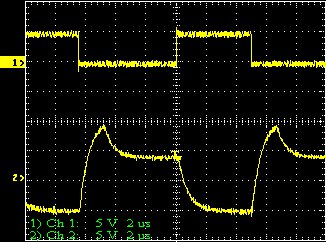
These timing diagrams are equivalent to the previous, but this time
the CCD is plunged into darkness. The video stage level comes closer to
the reference stage level, but it is still negative in comparison with
the ground.
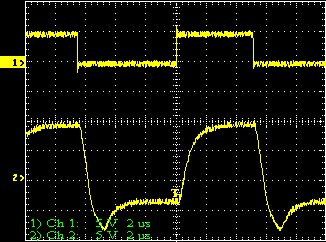
The following picture takes a close-up on the video signal according
to where it is measured in the amplifying chain. The TEST2
command is still used here.
Video signal on the pin 3 of U6, that is to say before the amplification.
The illumination conditions of the detector make the signal fill half the
useful dynamic. By examining the code of the TEST2
routine, you will notice that the reset stage duration is equivalent to
an OUT assembler instruction, whereas the reference
and video stage duration is equivalent to 3 OUT
instructions (the horizontal scale is 2µs/cm).
Signal on the pin 1 of the U6, after an amplification of about 15.
The limitation of the amplifier gain-band product is at the origin
of the clock edge smoothing. Lets notice that the reference and video
stages are established after about 2 µs. So it is necessary to wait
at least this delay to digitize the video stage after the rising edge of
the command signal P3.

Signal on the pin 7 of U6. The look of this signal is very close
to the previous one. Indeed, the clamping circuit gain is unitary, and
the bandpass is maximum. Lets notice that the routine TEST2
does not generate the clamping signal : the clamping capacitor C25 is then
shown like any other coupling capacitor. The signal still has an average
level close to zero.
Video signal on the pin 8 of U6. It settles at the output of the
last amplifier stage, which is a unity gain inverter. The video stage has
now a positive level compared to the ground.
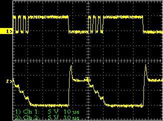
The following picture shows the video signal during the CCD
reading in binning 1x1. To observe it, you just have to launch a 0
second exposure with the PISCO graphic interface, or to execute the command
GLP
0 from the console and wait
for the READING status to appear.

Video signal on the pin 7 of U6 when the clamping is active. The
synchronizing signal is the P3. Lets check that the clamping had brought
the reference stage at the ground level (the arrow marked 2 on the left
of the frame). You can measure on this figure the point frequency of the
video signal when Audine acquires an image. It is about 26 kHz. The lengthening
of the video stage compared to the other stages is partly due to the conversion
time of the CAN and to the transfer towards the computer.

Video signal observed in the same conditions as before but this
time in 2x2 binning (Notice the look of the clock P3). The charge
storing effect is well visible in the video signal (the video stage disconnection
of the video stage which amplitude is twice at the end).
Same thing as for the previous picture but with a 4x4 binning.
The following timing diagrams show the some clock synchronization.

Above, the P3 clock command (equivalent, amplitude more or less,
to the clock H1 applied to the pin 7 of the CCD). Below, the clock R measured
on the pin 5 of the CCD. The command TEST2
has been used to produce this timing diagram.

The signal R/C (beginning of the CAN conversion) taken on the pin
24 of U5 (above) compared with the video signal (below). Notice that it
is necessary to wait about 6 ms before digitizing
the video signal, to let it enough time to be well established.

Position of the clamping signal compared with the reference stage.
The top is taken on the pin 11 of U4 (signal P5), arrives after a bit more
than 7 ms to be sure that the reference stage
is correctly established. The video signal is taken on the pin 7 of U6.
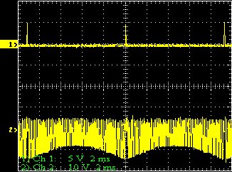
By using the PISCO TEST2 command and
the signal P1 as a synchronization, you can observe the video signal along
a whole image line. The video signal (below) is measured on the pin 7of
U6 and is synchronized by the signal P1 (above), taken on the pin 1 of
U5.The rounded aspect of the signal betrays a non uniform illumination
of the CCD during the integration period (a piece of black adhesive tape
was stuck on the CCD window, which caused a more important illumination
on the CCD sides than on its center).

Detail of the previous figure, around the end of the reading
of a video line and the beginning of the reading of the next one. Lets
notice the double impulsion of the signal P1 which is equivalent to the
clock V1 (amplitude more or less). The hidden pixels, and non electrically
connected, are very well visible at the beginning or at the end of
the line.

This timing diagram shows the video signal (pin 7 of U6) at the
beginning of the image line, but on a larger area than on the previous
view. In this case, the binning is 1x1. To do that, start an exposure in
a pronounced half-light and examine the video signal when the READING
status appears on the screen (you have at this moment about fifteen seconds
to analyze it). The end of the previous line is characterized by a high
cadence reading of the horizontal register, without digitizing. If you
glance
at the CCD low level reading functions, you will notice that this phase
corresponds to a cleaning cycle of the horizontal register, before this
one receives the content of the next image line. At the beginning of the
read line, the first pixels are quickly eliminated because we are not interested
in them. The actual digitization of the image points is realized just afterwards.

Here is the video signal at the beginning of the line whereas the
cleaning cycles are in progress (it happens when the RAZ status appears
on the screen). Notice that 4 image lines are accumulated in the horizontal
register before this one is read, in order to accelerate the proceedings.
The following figures show the look of the clocks edges applied to the
CCD.

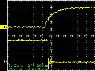
Rising time of the clock H1 (below) measured on the pin 7 of the
CCD (of course this one is at its place). The rising time is about 90 ns.
The synchronization signal is the command P3 (pin 1 of U4). The TEST2
command was used to produce this timing diagram.

Falling edge of the clock H2, observed on the pin 8 of the CCD (the
falling time value is 80 ns). The synchronization signal is the same as
on the previous figure : the crossing position of clocks H1 and H2 can
be analyzed. It appears approximately at 50% of the clock amplitude (this
is the optimal crossing point). Lets notice the delay of H2 in comparison
with P3, due to the propagation of the signals in the MAX333A.

The rising time of the clock V1 (pins 22, 21, 16 and 15 of the CCD)
is about 1 µs. The synchronization signal is the signal P1, taken
on the pin 1 of U5. The TEST command is used
to produce this timing diagram.

Falling time of the clock V2 ( pins 20, 19, 18, 17 of the CCD).
The synchronization signal is P1 (the same as for the previous figure).
Notice how the clocks V1 and V2 cross compared with the previous figure.
Above, the signal C1:2 (TTL type) from the PC whereas the link cable
PC/camera is 5 m long. Below, the same signal, but after its transit through
the trigger 74HCT14 (taken on the pin 4 of U1). The trigger returned stiff
edges for the command signals coming from the PC printer port.