
The transfer of charge into the different registers of the CCD requires a precise timing sequence. In addition to synchronization, however, the clocks must fulfill other requirements, among the most important being the high-level voltage, the low-level voltage and the rise and fall times of the clock waveform. Signals from the computer are in TTL logic, taking values of 0 volts and +5 volts approximately, depending on the logic level. Such signals are poorly adapted for controlling charge transfers and therefore an additional circuit has to be inserted between the computer and the CCD in order to produce the correct clock timing sequence. The clock circuit of a CCD behaves like the input of a MOS capacitor. It exhibits a parasitic input impedance that can reach a relatively high value (several nanofarads). During a change in logic state the timing circuits have to generate a sufficiently high current in order to produce clean, sharp edges to the waveform (at the instant of change the CCD is effectively in short circuit). If this current is not high enough the leading edge of the clock waveform becomes too rounded and this can cause the CCD to stop functioning. Once the logic state is reached, there is no problem since the input impedance of the CCD's timing circuit is very high. In order to achieve the correct shape to the clock waveform, we employ specialized circuits known as drivers.
CMOS IC drivers have not been chosen to produce the timing waveform for the Audine camera. Instead, we use signals produce directly by the computer to control analog switches. These devices switch the voltages required for the CCD to operate. We have chosen the IC MAX333A from Maxim which consists of 4 independent switches. This IC can switch voltages up to +/-20V. With its internal resistors, the MAX333A provides effective generation of clock signals with sufficiently steep leading edges.
The principle of an analog switch is very simple. The required logic level for the clock is obtained by successively switching the device between two distinct and different voltage levels. The voltage levels take values determined by the high and low levels required for the clock. The selection of one or the other of the voltage levels is controlled by the state of a logic signal coming directly from the computer's printer (parallel) port. The figure below shows how to wire one of the switches of the MAX333A IC to produce the vertical transfer clock sequence for the KAF-0400.

When the control signal (pin 1) is low, the clock signal available at pin 3
is at -8V. When the control signal is high, the clock signal at pin 3 is at
+0.5V. By alternately varying the logic state of the control signal it is therefore
straightforward to generate a clock waveform varying from +0.5V to -8V.
Electric charges from each pixel are sent one by one to the output stage of
the CCD at a frequency determined by the computer-synthesized clock timing sequence.
At the output stage the charges are converted into a voltage. This voltage,
which is present at a pin on the CCD chip, is then amplified by an external
circuit, and then digitized. This series of voltage levels is known as the video
signal (see diagram below).
In the KAF-0400, charge-to-voltage conversion is carried out by an amplifier
having a very high output sensitivity (charge-to-voltage conversion factor)
of 10 µV/e-.
The video signal is represented in the figure below:

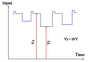
Point A in the diagram above is the top of the reset which corresponds to the pre-charge state of the floating diffusion in the output stage. When the switch from the pre-charge circuit opens, this causes a difference in voltage level due to parasitic capacitative coupling, and the signal falls to level B. Level B is known as the Reference level. At C, the information contained in a charge packet is sent into the floating diffusion. At a certain point, the video level D is reached. The voltage difference between the Reference level and the video level is directly proportional to the number of charges contained in the pixel that is being analyzed. We therefore need to extract this voltage difference. The figure below shows one possible way to carry this out. The amplitude of the video signal is measured with respect to ground. The signal Vr (the Reset level), then the signal Vi(the video level) are then measured. Then the difference Vi-Vr is calculated. The value of Vi-Vr is close to 0 Volts approximately, when the CCD is not illuminated, and Vi-Vr reaches about 1Volt when the CCD is saturated.
In practice, the presence of a superimposed dc component on the video signal of about 10V poses a problem, because it prevents the amplification of the difference voltage signal Vi-Vr of the right amplitude before digitization.
Fortunately it is easy to eliminate the dc voltage component by adding a capacitor C at the video signal output point, creating a capacitative link.


After the CCD a conventional RC filtering circuit (capacitor C1 and resistor R1) is inserted, which filters the dc component of the signal. This is our capacitative link mentioned previously but modified somewhat in order to improve the time constant that is proportional to the product R1xC1. The values indicated in the above diagram are characteristic for a pixel read-out frequency of several tens of kHz, which is typical for an astronomical (i.e. slow scan) CCD camera. If for any reason it is necessary to increase the time constant of the circuit, adjustments to the value of C1 are to be preferred over changes to R1, since leakage currents from the op-amp IC1, passing through this resistor, can give rise to offset voltages that can cause problems.
The first op-amp IC1 carries out the amplification of the signal. The gain is given by the formula:
G = 1+R3/R2.
The capacitor C2 and the analog switch IC perform the actual function of the clamping circuit. Once the Reference level for a given pixel is achieved, the switch closes for a brief instant (1-2 ms). This forces the potential of the Reference level with respect to ground. The switching cycle open/close/open is known as the "top" of the clamp. After the top, ground potential is maintained until the video level is achieved in its turn. Capacitor C2 allows this varying voltage to pass. Thus, the potential measured after C2 is equal to the voltage difference between Reference and video levels. The whole cycle begins again with the arrival of a new Reference level from the next pixel and the setting of the top of the clamp. Three conditions are required for everything to work correctly:
1. When the switch is closed, the circuit potential before C2 must have a minimum resistance so that ground potential is achieved. For this to be the case, op-amp IC1 must have an output resistance (or impedance) as low as possible and provide sufficient current to charge C2.
2. For the same reason as before, the resistance of the analog switch has to be very low when the switch is in the closed position.
3. When the switch is open, the output capacitance has to be isolated so that no significant discharge occurs with time. For this reason, amplifier IC2 is added at this point (it has a gain of 1). This op-amp has a very high non-inverting input impedance (+).
There is also a third op-amp (IC3) included in the circuit, of unit gain (R4=R5), its function being to invert the video signal so that it will increase in a positive sense with increasing light intensity.


The clamping circuit is attractive here since it is simple, employing as it does relatively few and readily available electronic components. We have used the MAX333A since a good quality clamping circuit can be based on these switches.

The video signal is analog in nature, and therefore has to be converted to a digital signal. This function is accomplished by an Analog-to-Digital Converter (ADC). On one side, the analog signal needed to be measured, coming from the op-amp, is applied to one of the pins of the ADC. On the other side, translated binary data resulting from the conversion are available on as many pins on the ADC as there are bits in the binary number produced. There are a wide variety of techniques for performing analog-to-digital conversion. The most popular is known as the method of successive-approximations, and is based on estimating the analog signal by successive weighting and comparing the input signal against a reference voltage.
An ADC can only determine an approximate value for the analog input signal. The converter precision depends in part on the resolution of the device. Output signals from an ADC being binary in nature, the resolution will be based on a power of 2. For example, if conversion is made with 15 bits (215 = 32768 ADU - Analog Digital Units). If the range in the analog signal input in the ADC is 10 Volts, the resolution will therefore be 10/215 = 0.30mV. The resolution of the ADC expresses the uncertainty in the voltage that is found between one quantification step and the next. Analog-to-digital conversion is always carried out after the amplification of the video signal. Thus to determine the resolution at the output of the CCD, the gain of the amplifier has to be taken into account. If the amplifier gain is equal to 16, the value of a single conversion step at the CCD output will be 0.15/16 = 9mV. The output sensitivity of the integrated amplifier in the KAF-0400 is equal to 10mV/e-; a single conversion step is therefore equivalent to a signal of 9/10 = 0.9 electrons.
In addition to resolution, the conversion time is also an important characteristic of the ADC. The conversion directly affects the read-out time of the CCD array. The Analog Devices AD976, chosen for Audine, performs a 16 bit conversion in 10 microseconds. The converter is a bipolar type, being able to convert a voltage range that has both positive and negative values. In Audine we only use the positive voltage range of the device, and the video signal conversion is performed with 15 bit precision (the dynamic range of the ADC is divided by two).
The AD976 IC is a simple but high performance device. It can perform a 16-bit conversion at a frequency of 100 kHz (200 kHz for the AD976A version). In addition, it only requires a drive voltage of +5V. Both a reference voltage and sample-and-hold functions are integrated on the chip thereby keeping the number of external components to a minimum (a sample-and-hold circuit is a circuit that can "freeze" the voltage to be measured during the conversion step). Linearity over the full dynamic range is +/-2 ADU. At the output, the data can be read over the full 16-bit range, or via a 2 x 8 bit multiplexer. Note that the integrated circuit ADS7821 from BURR BROWN is equivalent to the AD976, and is pin to pin compatible.
The following figure shows how to use the AD976 to send a 16-bit word over only 4 wires (1 nibble). The 8 multiplexed outputs from the AD976 have to be sent to an additional external 8-to-4 multiplexer, the 74HC157. When SELECT (pin 1) is low, inputs 1A, 2A, 3A and 4A are copied to output pins 1Y, 2Y, 3Y and 4Y. When SELECT is high, inputs 1B, 2B, 3B and 4B are output. By combining the signal MULTI1 with signal MULTI2, which control the multiplexing of the ADC (8 most significant bits or 8 least significant bits), it is possible to shift a 16-bit word in four steps of 1 nibble each.

|
|
|
|