
First, the optoelectronic performances; the main characteristics are summarised in the following Table.
|
|
|
| Optical form factor | 100% |
| Sensitivity @ 550 nm | 740000 e-/µJ/cm2 |
| '' | 37000 e-/µW/cm2 |
| '' | 146 mA/W |
| '' | 44.5 ke-/lux |
| Output Charge to Voltage Conversion Factor (CVF) | 10 µV/e- |
| Blue quantum efficiency @ 400 nm | 0.03 |
| Green quantum efficiency @ 550 nm | 0.33 |
| Red quantum efficiency @ 700 nm | 0.40 |
| Near IR quantum efficiency @100 nm | 0.08 |
| Reading noise | 13 electrons |
| Dark current density @ 25°C | 10 pA/cm2 |
| Dark signal | 50 e-/pixel/s |
| Signal level at saturation | 0.11 µJ/cm2 |
| Dynamic range | 76 dB |
| Non-linearity | 1% |
Kodak gives the sensitivity expressed in various units. But it is to be noticed that the sensitivity figure is largely dependent upon the wavelength. By a footnote Kodak indicate that the figures of the table are valid for 550 nm wavelength.
It is not too difficult to convert one unit in another. As example, knowing the power, expressed in Watt, the energy expressed in Joules is the power (in Watts) multiplied by the time (in seconds). Thus 1 Joule = 1 Watt*1seconde. It results :
Kodak considers the case of the use of the CCD in video mode (called
CCIR mode) with an integration time of 20 ms (0.02 second). Those units
express the signal in electrons versus illumination.
The computation of the sensitivity in Volt/µJ/cm2, is more usable
than e-/µJ/cm2. The conversion is very simple knowing
the Charge to Voltage conversion Factor (CVF). Kodak gives a typical figure
of 10 µV/e- for the CVF.
Thus the sensitivity in Volt/µJ/cm2 is :
In the case of the KAF-0400 :
Concerning the e-/lux, it's a monster ! The lux is the lighting unit for a photo-visual radiation (visual domain centred around 550 nm). But the accurate definitions of the lighting conditions (luminance of the source, temperature of colour, potential filters) are not specified. It results confusions with this unit, perfectly unable to accurately characterise the sensitivity of a CCD to be used in astronomy. The problem is that some of the CCD manufacturers (in particular component manufacturers for small video cameras at low cost) only specify their CCD with this unit. Normally, 1 lux is equal to an illumination power flux density of 1.47.10-7 W/cm2.
To try to translate the sensitivity in µJ/cm2 at 550 nm, the following formula has to be used :
The quantum efficiency (ratio between the number of incident photons to the number of produced electrons) at a given wavelength is given by :
The Table below gives the dark signal versus temperature in the range
generally used by amateur CCD astronomy.
|
|
|
|
|
|
|
|
|
|
|
|
|
|
|
|
|
|
|
|
|
|
|
|
|
|
|
The data sheet doesn't specify that the announced dark signal is a mean figure. Actually, some of the pixels are affected by a dark current 10 or 100 time higher than the mean value. An exposure in the dark of a few seconds, at the ambient temperature, shows perfectly the abnormal pixels. They are called 'hot pixels'. Fortunately, it is relatively easy to correct this defect by a few elementary image processing operations. .
The dynamic is a very important parameter for astronomy being given the luminosity discrepancy existing between objects on one CCD image, from faint arm of galaxy just above the noise to bright stars in the field of view. The optical signal driving the CCD to saturation is Esat is equal to 0,11 µJ/cm2. As the response of the CCD is 740000 e-/µJ/cm2, It is easy to compute the number of electrons the potential well of each pixel can reach before leaking in the adjacent pixels :
It worth noting that the saturation level of the horizontal register is twice (170000 e-) that of vertical register. This allows the binning with a factor of 2 in the horizontal register (adding 2 consecutive lines in the horizontal register). In addition the output register saturation level is four time (340000 e-) the one of the vertical register. From this nice arrangement, it results that the KAF-0400 can efficiently be used in 2*2 binning mode.
1% non-linearity is a typical figure for CCD.
After this introduction to CCD, stating from the data sheet of the CCD manufacturer, this page presents the core of the component : the internal architecture of the CCD. A user-oriented view of the CCD is enough to evaluate how to use the CCD for astronomy. For KAF-0400, the architecture is simplified due to the absence of memory zone and to the two-phase mode for the charge transfer. Nothing very complex to set up this component. The KAF-0400 internal organisation informs us the image area includes 520 lines and 784 columns. 4 line at the top of the image and 4 lines at the bottom are covered by a mask and used as dark signal reference, similarly 16 columns, 4 at the beginning and 12 at the end of the video line, are used as dark signal reference or electrical reference. The KAF-0400 includes a horizontal register of 784 pixels and an output stage with a floating diode with its associated pre-charge network. .

The name of the different clocks, their functions and their nominal
electrical characteristics are given in the following table :
|
|
|
|
|
|
|
|
|
|
|
|
|
|
|
|
|
|
|
|
|
|
|
|
|
|
|
|
|
|
|
|
|
|
|
|
Kodak mentions a 24 nF capacitive load for each horizontal clock. It's rather high. By chance two effects alleviate the potential deleterious effects of this capacitive load on the raise time of the clocks. In one hand, for astronomy, the single shot picture make a rather slow reading of the CCD, allowing the clocks to raise up acceptable. In the other hand, after experimentation, the 24 nF figure look rather conservative for the KAF-0400, probably to maintain the full compatibility of the interface network with its cousin the KAF-1600. In fact, for the KAF-1600, there are twice as much lines and columns as for the KAF-0400, and thus the capacitance per phase is about twice the one of KAF-0400. For the KAF-0400, the capacitive load is estimated to about 10 nF. This allows to use analogue switch drivers. The capacitive load of the other clocks is in the range of 100 pF for H1 and H2 and 5 pF for R, this means they are small enough to have no problem at all on the shape of the clock signals.
Kodak doesn't give any information about the crossover level of the clocks. We have designed the clocks for a crossover at mid-voltage between the two levels.
Between two successive transfers of a line of the image into the horizontal register, the whole horizontal register must be shifted and read. One CCD line consists of 10 non-active pixels (not linked to a photosite), 4 masked pixels corresponding to the 4 masked columns explained just above, 768 useful pixels of the image and 12 masked pixels corresponding to the 12 masked columns on the other side of the image. It results, 794 clock periods, at the minimum, have to be sent to empty the full horizontal register.

Take care to have at least the minimum duration for the pulses of the clocks is of primary importance for efficient charge transfer. A longer duration doesn't disturb the charge transfer mechanism. Insertion of small delays by software between each step in generating the clocks allowsachieving this delay. As an example, the following code lines generate the V1 and V2 clocks :
//
bit 0 of the output port is linked to V1 clock
//
bit 1 of the output port is linked to V2 clock
outp(DATA, 0x00);
// bit 0 set to 0 and bit 1 set to 0
outp(DATA, 0x00);
outp(DATA, 0x00);
outp(DATA, 0x01);
// bit 0 set to 1 and bit 1 set to 0
outp(DATA, 0x01);
outp(DATA, 0x01);
outp(DATA, 0x01);
// bit 0 set to 1 and bit 1 set to 0
outp(DATA, 0x01);
outp(DATA, 0x01);
outp(DATA, 0x02);
// bit 0 set to 0 and bit 1 set to 1
outp(DATA, 0x02);
outp(DATA, 0x02);
outp(DATA, 0x01);
// bit 0 set to 1 and bit 1 set to 0
outp(DATA, 0x01);
outp(DATA, 0x01);
outp(DATA, 0x00);
// bit 0 set to 0 and bit 1 set to 0
outp(DATA, 0x00);
outp(DATA, 0x00);
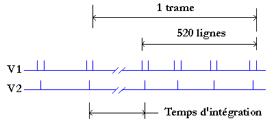
The next Figure shows the timing diagram of the V1 and V2 clocks to read a full image. The full reading time, (sometime including the exposure) is called a frame. The CCD consists of 520 lines. 4 lines at the top of the image and 4 at the bottom are masked to the incoming light. They may be used for dark current correction. (The AUDINE camera doesn't use this capability, but you can do something with these masked pixels).
The next Figure shows the timing diagram of the clocks to provide the charges transfer in the horizontal register. Three clocks are involved H1, H2 and R. The reference level of the video signal is available at the going down edge of the H1 clock. The video signal is available while H1 clock is high. Take note of the synchronisation of the R clock with H clocks. The R clock may be a very short pulse (a few nanoseconds is enough). As the performance of the parallel interface is in the range of a few hundred of kilo-Hertz, we are far from the limit of the horizontal register and of the output amplifier, they can be red with clocks at several mega-Hertz. Using slow H1, H2 and R has the advantage to allow more time for establishing each level. This results in a noise reduction.

It is possible to modify the nominal timing diagrams of the clocks to achieve some specific mode of operation of your CCD. This type of experimentation should not endanger the life of your CCD. Hereafter is an example. It is the case of the binning mode on the two axes. It is very important for CCD astronomy it allow to combine the pixels by four, doubling the size of the pixel and thus reducing the size of the image file. We proceed in two steps. First, we add two consecutive lines in the horizontal register before reading it. Second a reset pulse is generated only each two consecutive pixels (this is equivalent to make the sum of the two pixels into the output diode). The same result could be obtained reading at full resolution the CCD and making the binning addition by software. Then, we would lose two of the main advantage of performing the binning in the CCD sensor: divide by 4 the time to read the image, and divide by 1.414 the reading noise with respect to an addition by software of the four pixels.


|
|
|
|