The interface network |

The power conditioning network |

The clock shaping network |
The clock levelling networks |
The CCD network |
The amplifier network |
|
The interface network |
The power conditioning network |
|
The clock shaping network |
The clock levelling networks |
|
The CCD network |
The amplifier network |

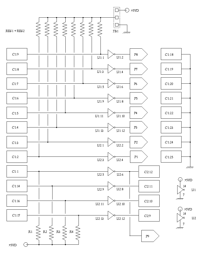
All the command bits are shaped by the 74HCT14 (U1 and U2) triggers and the pull-up resistors network (or pull-down, depending of the position of the TB1 contact). The cable between the PC and the camera must be a ribbon of twisted pairs.(Between two signal lines there is a ground line). The maximum length for the cable is approximately 7 meters.
All the basic control functions of the camera can be done on eight bits. These bits are generated by the printer port of the PC (pins 2 to 9 of DB25 connector). 4 additional bits coming from the PC, are unused and left free for future extensions. For example, these free bits can be used for shutter and/or filter wheel commanding or for an electronic multiplexer allowing to command several AUDINE cameras simultaneously. (One PC could command a camera for the image acquisition itself, another for auto-guiding, and why not, another as a view-finder...)
The four unused bits come out of the camera on the on the DB15 connector.
Hereafter is the pin description of the DB15 connector :
|
|
|
|
|
+15V (electronic) |
|
|
Ground (electronic) |
|
|
-15V (electronic) |
|
|
+5V (Peltier) |
|
|
+5V (Peltier) |
|
|
Ground (Peltier) |
|
|
Ground (Peltier) |
|
|
+12V (fan) |
|
|
Command (Select In) |
|
|
Command (Init) |
|
|
Command (Auto Feed) |
|
|
Command (Strobe) |
|
|
Ground (electronic) |
|
|
Reserved |
|
|
Reserved |
Pins 14 and 15 are linked to the TB3 connector of the upper board. They can be used, for example, to add a thermal probe to the camera.
Note: The 74HCT14 IC (Integrated Circuit) inverses all the bits.
The command signals are renamed from P1 to P8 at the outputs of the
triggers. The functions of these signals are as follows :
|
|
|
|
|
V1 Clock |
|
|
V2 Clock |
|
|
H1 et H2 Clock |
|
|
R Clock |
|
|
Clamping Clock |
|
|
A/D converter control command |
|
|
CAN multiplexing |
|
|
74HCT157 multiplexing |
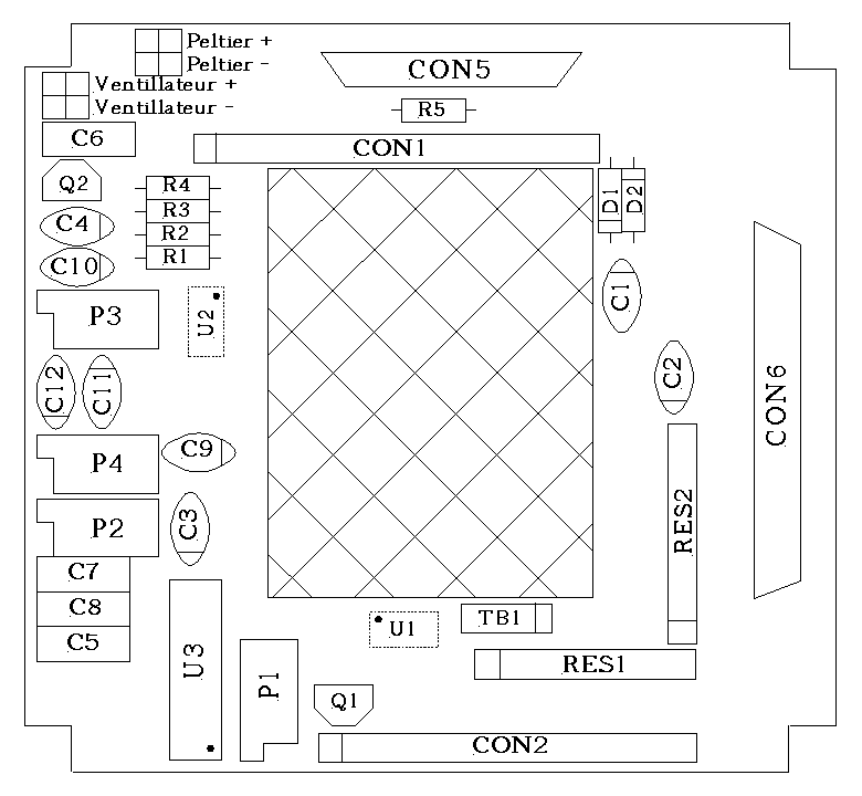
The power supply of the electronics is +/-15V. (It is possible to supply the electronics from +/-18V using the small adaptation explained here below). The required currents to feed the electronics of the camera are : 60 mA out of +15V and 20 mA out of -15V. Two78L05 (Q1 and Q2) regulators deliver two +5V supplies. One is for the analogue circuits and the A/D converter and the other one is for the digital circuits. The diodes D1 and D2 protect against polarity inversion of the power supply.
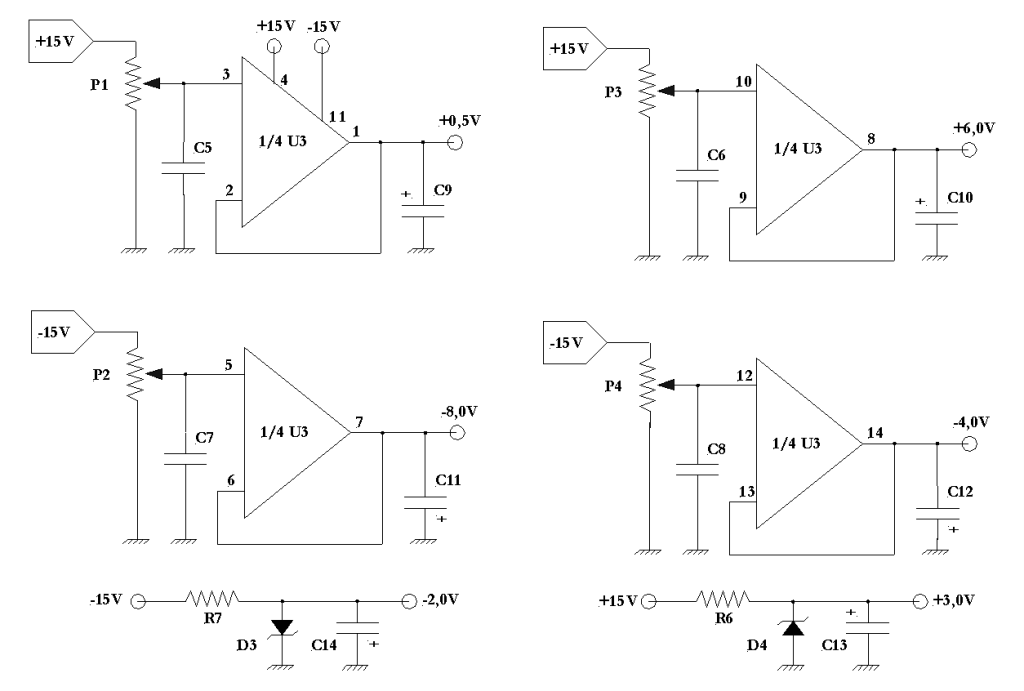
The LM348 (U3) IC comprises four operational amplifiers. They are use to supply some of the clocks (V1, V2 and H). Potentiometers (multiturn trimming potentiometers), located on the lower board, allow clock level adjustment.
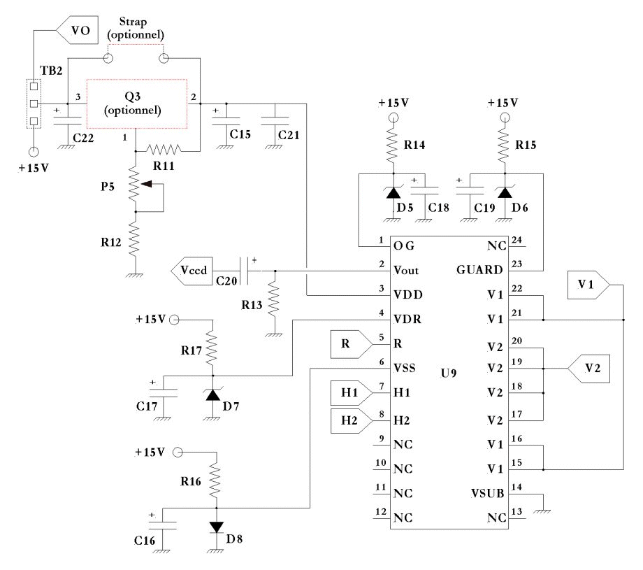
The two IC's U4 and U5 are MAX333A. The MAX333A is an improved version of MAX333. Either version may be used for AUDINE. No significant difference of image quality results.
Zener-diodes generate the various voltages necessary to the CCD (VDR, VSS, OG, GUARD). The case of VDD voltage is a case apart (This supplies the voltage of the amplifier integrated within the CCD). It is possible to get VDD directly from the general +15V, or to add a LM317 (Q3) regulator. This allows the camera to work from +/-18V supply. In this case, the P5 potentiometer has to be trimmed so that the voltage at the pin 3 of the CCD mount is +15V. The part of the documentation explaining how to assemble your camera gives additional information about the advantages and the drawbacks of the two options.
For both of the options, you can switch off the voltage of the amplifier within the CCD while it is integrating the image. (For this purpose, one of the reserved lines (pin 14) of the DB15 connector may be used). The reasoning behind this is to completely eliminate electroluminescence produced by the amplifier of the CCD during integration. This procedure is an option; it is not yet implemented in the software driving the AUDINE camera. Presently, the amplifier is permanently supplied but with a lower voltage than specified by Kodak. It's another way to cancel electroluminescence. (See the configuration of the TP2 selection switch mounting the upper board).
The video signal is available on pin 2 of the CCD. The R2 resistor loads the output amplifier. The C1 capacitor cancels the DC component.
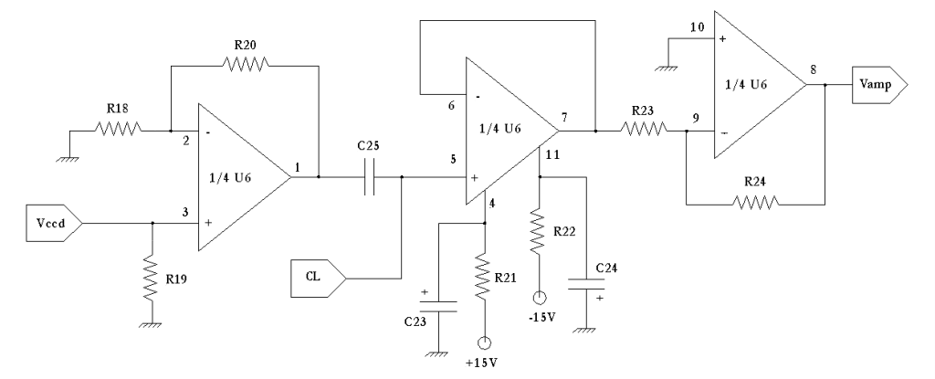
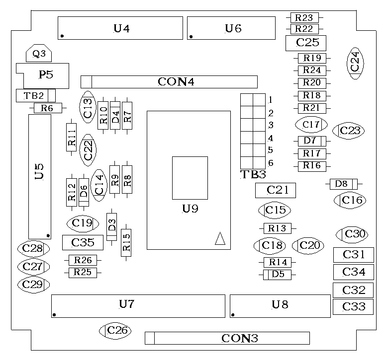
The signal processing chain includes three BiFET amplifiers (out of the 4 included in the AD713 (U6) IC). The reference level is put to the ground by a clamp network. The clamp capacitor is C11 and the clamp switch is one of the switches of the MAX333A (U4) activated by P5. The gain of the signal processing chain is about 16 times.
The amplified signal goes to the input (pin 1) of the analogue to digital converter AD976 (U7) IC. This IC comes in two versions : the AD976, performing 16-bit conversion in 10µs, and the AD976A, with a 16-bit conversion in 5µs. Obviously, the second version allows a shorter reading time of the CCD. But, considering the limitation in clock cycle generation, the overall reduction in the reading time would be only 10%. This is why AD976 is used for AUDINE. The supplies of this IC are carefully filtered (C28, C29, C35). The conversion starts on the falling edge of the R/C signal (command P6). After completion of the A/D conversion, (managed by a software waiting loop), the BYTE signal (command P7) is used to select from the 16-bit word, either the 8 least significant bits (BYTE at low level) or the most significant bits (BYTE at high level). The bits are output at pins 15 to 22. Beware ! There is a trap. The data available at the output of the ADC is actually the result of the previous conversion. Usually, this fact is not a problem, but sometimes it is important to keep this in mind. For example, the first valid digital data in the video line is only obtained after two conversions. The impact of this specificity can be even trickier in case you want to perform a correlated sampling with a double digital conversion; (it's possible with AUDINE). Then you have to take care to put the 16-bit words in the right order before subtracting.
The74HCT157 (U8) IC is a multiplexer used to transfer the digital image in 4-bit groups to the PC. The filtering capacitors C21, C22, C23 and C24 improve the transmission.
|
|
|
|