
The electronic diagram of the supply network of the CCD output amplifier. It shows the two important options discussed in this page : either wiring Q3 regulator or simply replacing it by a strap (a wire).
First, we see a two-position switch, TB2. It is used to select either the +15V or the VO supply voltage. The VO is also +15V voltage, it comes from the +15V main bus through an analogue switch of the U5 IC (MAX333A). This switch, driven by the computer, switches off this voltage when supply of the CCD output amplifier is not needed, in particular, during the integration time of the CCD. This avoiding the electroluminescence phenomena (the CCD internal output amplifier may emit a very faint light over the sensitive area, which would be worrisome in long exposure images). The electroluminescence risk is reduced in the AUDINE design by supplying the amplifier with a voltage slightly lower than nominal (see explanations hereafter). With the present version of AUDINE and the associated acquisition software, it is recommended to set the switch in the +15V position (it's a simple wire-staple switch).
Second, an important alternative :
|
|
|
| It is possible to supply the camera with a power supply other than +/-15V (slightly higher). For example, you can use a +/- 18V power supply and adjust the P5 potentiometer so that +15V is effectively delivered to the pin 3 of CCD. | If you supply AUDINE with a +/-15V power supply (easy to find and cheap), the delivered voltage VDD will be significantly lower than the +15V specified. The protection diode D1 produces about 0.7V voltage dropping, then the regulator produces 1.6V dropping, even if the potentiometer is set so that the LM317 doesn't produce any regulation. With a +15V power supply at the input of the camera, the VDD voltage will be 15-0.7-1.6 = 12.7V. That is rather below the +15V nominal voltage. With this voltage AUDINE continues to operate, but it is at the limit (as shown hereafter). This problem is serious enough to reject the Option 1 if you wish to use a +/- 15V general power supply for the camera. |
| As a solution for powering the electronics of the camera you can use 4,5V-batteries (2 x 4). If you don't need to cool the camera, (example: for planetary imaging or telescope tracking correction); this is a simple solution to be independent of AC power supply. | |
| If the general power supply is not very good, the LM317 stabilises the voltage. In fact, a variation of the VDD voltage during the readout of the CCD can create horizontal spurious in the image. |
|
|
|
| If you use a +/- 15V general power supply, the VDD voltage
is about 14.3 V. (The power supply voltage less the D1 voltage dropping,
about 0.7 V).
The small undervoltage of the amplifier is an advantage, it reduces the electroluminescence risk of the amplifier without significantly modifying the performance of the amplifier (see diagrams hereafter). |
The CCD output power amplifier is not protected against contingent overvoltage. Kodak specifies +16V as maximum limit for VDD. Higher voltage may damage the CCD. If it's a real risk, Option 1 is recommended. Option 2 implies the use of a fixed-voltage regulated power supply for the AUDINE electronics (not a button-adjustable output power supply, the button could be turned inadvertently). Thus the power supply has to be a +/-15V one. |
| The stability of the power supply has to be good so that it doesn't affect the image quality (less than 2mV RMS fluctuation, stability of the same order of magnitude over 15 seconds). | |
| It is not possible to directly use a battery as a power supply. It is necessary to produce stable regulated +/- 15V supplies using regulators between the battery and AUDINE (7815 and 7915 IC are convenient). |
Cost, ease of utilisation and performances are parameters in favour
of Option 2.
The small +/-15V power supply, AL890N from ELC S.A. (59, avenue des Romains,
74000 Annecy) is recommended. It is available in France at most electronic
shops for about 300 FF (US$ 50) (VAT included). The voltages are fixed,
so there is no trimming at the setting up. The power supply is of linear
type and the manufacturing quality is good. Finally, the CCD point of operation
is nearly nominal as shown hereafter.
The next diagram shows, versus the VDD voltage, the ratio in electrons
per ADU (Analogue Digital Unit), i.e. the number of electrons required
for one least significant bit of the digital code. This is the result of
measurements made with one of the AUDINE cameras. The smaller is
this ratio; the better is the camera. There is serious malfunctioning of
the CCD with VDD below 12.5V. With VDD equal to 14.3V the ratio is very
near to the ratio with the nominal VDD voltage +15V.
It's worthwhile pointing out that the sensitivity of AUDINE is 1 ADU
for two electrons. It's rather high.

The second diagram, here below, shows the RMS readout noise expressed
in electrons versus the VDD voltage. As in the previous diagram, malfunctioning
appears for voltages below 12.5V resulting in an increased readout noise.
The RMS readout noise is around 18 electrons with VDD = 14V.

Now, we will see how to wire the AUDINE camera for Option 1 or Option 2.
Solder the voltage regulator Q3, an LM37 IC. It is packaged in a TO92 box with three wires. Already you have mounted this kind of component on the lower printed circuit board. Now you know how to proceed. Orient correctly the flat part of the component !

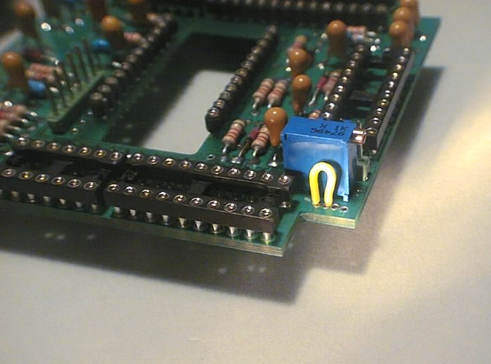
Solder 3 pins from the AMPMODU bar to constitute the TB2 switch. This switch selects either the direct link to +15V or the link through a commanded analogue switch for the supplying of the CCD internal amplifier. Near the switch mount, solder the 1kW potentiometer P5.


Wiring Option 2 is very similar to Option 1. Even if R11 and R12 resistors and P5 potentiometer are not necessary in this option, it is recommended to wire them just in case you comeback to the Option 1. The only difference with respect to Option 1 is to replace the regulator by a simple wire between the holes for pins 2 and 3 of Q3. With this wiring the CCD output amplifier is directly fed from the +15V or VO depending of the position of TB2. Wire TB2 switch as in Option 1.

Again, if you use a +/-15V fixed voltage power supply, the Option 2 is recommended.
|
|
|
|