The pins 9, 10, 11 and 12 of the DB15 (C2) connector represent a small footprint output port dedicated to external devices commanding for instance a telescope handpad (for autoguiding), a shutter, a filter wheel, another camera connected to the same computer... These pins can take two binary logical levels, 0V or +5V (those are the TTL output ports ! ?). The state of this 4-bits small footprint bus is very easily programmed by software. The computer receives the commands through the DB25 connector. At need one can for example use an elementary circuitry external to the camera to issue 16 command lines from the information available on the 4 pins of the port, which allows for numerous extension abilities.
Hereunder is displayed the summary of the control registers of the printer port of a PC; these allow to drive the output port (if P is the base address of the printer register, the control register is at P+2).
|
|
|
|
|
|
|
|
|
|
|
|
|
|
|
|
|
|
|
|
|
|
|
|
|
|
|
|
|
|
|
|
|
|
|
|
The bits to be configured are D0, D1, D2 and D3. The bit D0 commands the pin 12 of the C2 connector, the bit D1 commands the pin 11, the bit D2 Commands the pin 10 and the bit D3 commands the pin 9. The ground is on the pin 2 of the C2 connector.
It should be noted that the signal present on the pin 11 of the C2 connector is also available from inside the camera on the pin 3 of TB3. This signal will preferably be used to drive a shutter device, which can then be at will internal to the camera housing, or external.
Let us illustrate the command bus programmation of the camera through an example. Accounting for the inverters 74HCT14 of the lower board (circuit U2), setting the pin 9 of the connector DB15 to the " up ", or 1 logical level (or the +5V voltage), one should write a program that does the following:
out P+2,8
To set this bit to 0 one must write:
out P+2,0
Generally speaking, in order to set the 4 signals of the Audine output port, one must write 1011 into the configuration control register, that is:
out P+2,11
On the other hand, to nullify those 4 signals one must write 0100, which is obviously done by writing :
out P+2,4
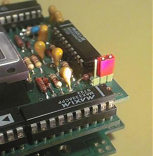
The D0 bit of the control register fulfills an additional function in the Audine camera: It allows to issue the P9 signal which commands the alimentation of the CCD's amplifier (VDD voltage). This functionality was foreseen to mandatorily avoid a possible electroluminescence problem from the amplifier built-in the CCD chip.. The idea is imply to not supply any power to the amplifier during the exposure then restore the nominal voltage a fraction of second before the image reading after integration. The D0 bit allows this provided that the TB2 strap has been set has shown on the image below (in this configuration, the VDD voltage goes through one of the free analog switches of the U5 circuit (MAX333A). Please note that this feature is totally independent of the option chosen to feed the amplifier.
The TB2 strap is set to authorize the software setting of the VDD voltage applied to the CCD chip. Please note that on this Audine board the P5 potentiometer is not wired, as it is not required if one chooses the option 2 (fixed VDD voltage out of the software-selected ON/OFF).
To power the CCD's amplifier one must write:
out P+2,1
and to switch it off :
out P+2,0
Warning: this possibility can conflict with the use of the the bit D0 (pin 12 of C2) while driving an external electronic device. In this case it is recommended to only use the bits D1, D2 and D3 to drive the system and reserve the sole use of the bit D0 to command the amplifier.
The two following pictures show that the possibility to shutoff the CCD's amplifier actually works on Audine. These are 2 images shot under darkness with the new CCD chip KAF-0401E which unfortunately includes a light amplifier (this light is very dim but sufficient to trigger the pixels in the vicinity of the amplifier). The exposure duration is in both cases 60 seconds and the CCD chip is moderately cooled. The reading is done in 2x2 binning.

At the top, an image shot while leaving the amplifier power-supplied
during 60 seconds of integration time in the dark (CCD chip KAF-0401E).
Hot points appear since the CCD chip is hardly cooled. The amplifier lies
in the lower right corner and the light that it generates can perfectly
be perceived.
At the bottom, the exposure still is 60 seconds, but here the amplifier
was not power-supplied during the exposure. It gets powered again by software
(here the PISCO software) only a fraction
of a second before the reading. The electroluminescence completely
disappears with this setup.
One configuration which can be considered as standard with Audine consists in reserving, as we just saw, the bit D0 to the commanding of the CCD amplifier.
The bit D1 of the control register (pin 11 of the connector DB15 or pin 3 of
the internal connector TB3) will be primarily reserved for the control
of a shutter.
The remaining bits D2 and D3 can be used to control
the telescope by simulating a serial port (electronic hand controller, autoguiding,
focus, ...).
|
|
|
|