
Part of the layout, showing the potentiometers place.
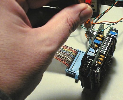
The potentiometers adjustment is achieved with a watchmaker screwdriver,
turning the tiny screw on the side. The whole excursion needs 20 turns
to be covered.
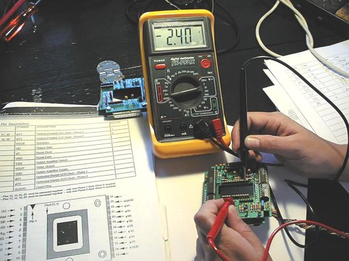
Begin by adjusting the high and low level of the clock applied to the CCD : this can be done through the 4 potentiometers set onto the inferior board. Then assemble the boards, connect them to the PC parallel port with the cable, and power all on. Start PISCO and execute the SET0 command with the console. By measuring the pin 7 voltage you find any value : your mission is to bring it close to +6.0V with the potentiometer P3 of the inferior board. This clock is fH : it performs the charge transfer within the horizontal register.
Part of the layout, showing the potentiometers place.
The potentiometers adjustment is achieved with a watchmaker screwdriver,
turning the tiny screw on the side. The whole excursion needs 20 turns
to be covered.
Turn the potentiometer P3 once and check the CCD socket pin 7 voltage. If you get closer to +6.0V then turn on in the same direction, else try the other one. Some iterations are often needed. This voltage doesnt need to be accurate to the hundredth of volt : few tenth are quite well. Thats finished for the fH high level.
Test now the CCD socket pin 8 : this represents the fH low level. Adjust the potentiometer P4 to bring it close to -4.0V.
The aim is now to adjust the level of the vertical transfer clock, namely V1 and V2. The CCD socket pin 22 represents the high level of these clocks : turn the potentiometer P1 to measure +0.5V. When done, check the pins 15, 16, 17, 18, 19, 20, 21 to be equal to this voltage.
The setting of the vertical clocks low level needs to execute the PISCO command SET255. The pins from 15 up to 22 (which are to the same potential) must be tied to 8.0V by adjusting the potentiometer P2.
The Reset clock range (pin 5) is set by Zener diodes : it cant be adjusted, but its good to check it. The command SET0 must produce a voltage about +3V whereas the command SET255 must bring it to about 2V.
The following table specifies the range of the high and low levels for
each clock, according to Kodak :
|
|
|
|
|
| High V1 level | 0.0V | +0.5V | +1.0V |
| Low V1 level | -8.5V | -8.0V | -7.5V |
| High H1/H2 level | +4.0V | +6.0V | +8.0V |
| Low H1/H2 level | -6.0V | -4.0V | -2.0V |
| High R level | / | +3.0V | +5.0V |
| Low R level | -5.0V | -2.0V | / |
Now we will check the DC voltages applied to the CCD. The first of them is VDD, pin 3 : it is adjustable whether you have chosen the option 1 for supplying the CCD output amplifier. In that case, and if you supply the camera with a +/-18V source, you must adjust the potentiometer P5 on the superior board to have a potential of 15V on pin 3. If you have chosen the option 1 but supply the camera with a +/-15V source, you cant have +15V : turn the potentiometer P5 to have the maximum value (which can range from 12.6V to 12.9V). The CCD will work, but not in nominal conditions.

But with the option 2, the VDD level is not adjustable, but should hang around +14.2V with a +/-15V power supply (any other kind of power supply is absolutely forbidden here).
The other CCD continuous voltages must be seriously checked despite
they are generated with Zener diodes.
Pin 1 is OG, must be close 3V.
Pin 4 is VDR, must be close to +10V.
Pin 6 is VSS, must be close to +0.7V.
Pin 23 is GUARD, and must be close to +7.0V
Pin 14 is the ground.
Pins 9, 10, 11, 12, 13, 24 are not connected.
The pin 2 is the output video signal. When theres no CCD, its level is about 0V.
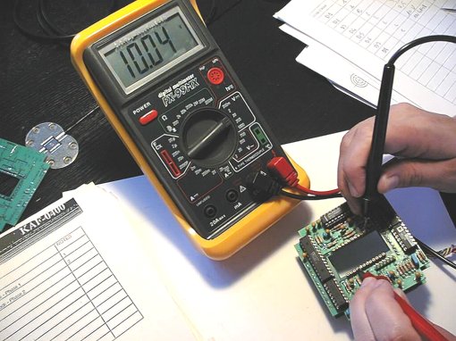
Measuring pin 4 VDR continuous level.
The hereafter table gives the continuous levels recommended by Kodak
:
|
|
|
|
|
| VSUB | 0.0V | 0.0V | 0.0V |
| VDD | +14.75V | +15.00V | +15.25V |
| VSS | +0.6V | +0.7V | +1,5V |
| VDR | +9.75V | +10.00V | +10.25 |
| OG | +1.0V | +3.0V | +5.0V |
| GUARD | +5.0V | +7.0V | +10V |
The next tables sum up the voltages to be measured on the CCD socket
after having executed the command SET0 and
SET255.
The nominal values are given, but also those measured on an manufactured
Audine, and then the values given by Kodak not to destroy the CCD.
|
|
|
|
|
|
|
| 1 | OG | +3.0V | +3.5V | +6V | -1V |
| 2 | Vout | Video signal | Video signal | / | / |
| 3 | VDD | +15.0V | +14.4V | +16V | -0.5V |
| 4 | VDR | +10.0V | +10.4V | +16V | -0.5V |
| 5 | R | +3.0V | +4.0V | +10V | -10V |
| 6 | VSS | +0.7V | +0.7V | +16V | -0.5V |
| 7 | H1 | +6.0V | +6.0V | +10V | -10V |
| 8 | H2 | -4.0V | -4.0V | +10V | -10V |
| 9 | No connected | / | / | / | / |
| 10 | No connected | / | / | / | / |
| 11 | No connected | / | / | / | / |
| 12 | No connected | / | / | / | / |
| 13 | No connected | / | / | / | / |
| 14 | VSUB | 0V | 0V | / | / |
| 15 | V1 | 0.5V | 0.5V | +10V | -10V |
| 16 | V1 | 0.5V | 0.5V | +10V | -10V |
| 17 | V2 | 0.5V | 0.5V | +10V | -10V |
| 18 | V2 | 0.5V | 0.5V | +10V | -10V |
| 19 | V2 | 0.5V | 0.5V | +10V | -10V |
| 20 | V2 | 0.5V | 0.5V | +10V | -10V |
| 21 | V1 | 0.5V | 0.5V | +10V | -10V |
| 22 | V1 | 0.5V | 0.5V | +10V | -10V |
| 23 | GUARD | 7.0V | 7.2V | +16V | -0.5V |
| 24 | No connected | / | / | / | / |
|
|
|
|
|
|
|
| 1 | OG | +3.0V | +3.5V | +6V | -1V |
| 2 | Vout | Video signal | Video signal | / | / |
| 3 | VDD | +15.0V | +14.4V | +16V | -0.5V |
| 4 | VDR | +10.0V | +10.4V | +16V | -0.5V |
| 5 | R | -2.0V | -2.4V | +10V | -10V |
| 6 | VSS | +0.7V | +0.7V | +16V | -0.5V |
| 7 | H1 | -4.0V | -4.0V | +10V | -10V |
| 8 | H2 | +6.0V | +6.0V | +10V | -10V |
| 9 | No connected | / | / | / | / |
| 10 | No connected | / | / | / | / |
| 11 | No connected | / | / | / | / |
| 12 | No connected | / | / | / | / |
| 13 | No connected | / | / | / | / |
| 14 | VSUB | 0V | 0V | / | / |
| 15 | V1 | -8.0V | -8.0V | +10V | -10V |
| 16 | V1 | -8.0V | -8.0V | +10V | -10V |
| 17 | V2 | -8.0V | -8.0V | +10V | -10V |
| 18 | V2 | -8.0V | -8.0V | +10V | -10V |
| 19 | V2 | -8.0V | -8.0V | +10V | -10V |
| 20 | V2 | -8.0V | -8.0V | +10V | -10V |
| 21 | V1 | -8.0V | -8.0V | +10V | -10V |
| 22 | V1 | -8.0V | -8.0V | +10V | -10V |
| 23 | GUARD | 7.0V | 7.2V | +16V | -0.5V |
| 24 | No connected | / | / | / | / |
If you dont have those voltages, the classic reason is having inverted a polarized capacitors (Tantalum drop capacitors). This produces a shortcut and drops the supplies down (regulators Q1 and Q2 might heat strongly : draw your finger near them to check). A wrong Zener diode, or mounting it in the opposite sense produce the same effects.
|
|
|
|